Engineering notes for anyone modifying the board, respinning it, or reviewing it.
For the student-facing guide see ../README.md.
- Design:
campv2/— KiCad 10.0, file format20260206 - Title block: TechnoCamp2026 Circuitry Class — schematic rev B, board rev B, 2026-08-09
- Outline: 80.0 × 80.0 mm, rounded corners, 1.6 mm FR-4, 2 layers, HASL
- Assembly: 100 % through-hole, single-sided placement except U1 (bottom)
- Vias: none. Every net is routed on one layer or reaches the other through a through-hole pad.
1. What this board is
A passive carrier for an Arduino Nano. There is no active silicon on the PCB — no regulator, no level shifter, no protection. The board contributes:
- A socket for the Nano and headers for four off-board modules,
- Six current-limiting resistors for two RGB LEDs,
- Three buttons wired for internal pull-ups,
- A jumper that reconfigures the RGB LEDs between common-cathode and common-anode,
- Power distribution via two copper pours.
Design intent is pedagogical: every net should be traceable by eye with a multimeter, and every part should be replaceable with a soldering iron.
2. Netlist
Extracted from campv2.kicad_pcb. Reference designators are as they appear on the
silkscreen (see §7 — they differ from the schematic).
Power
| Net | Pads |
|---|---|
VCC |
ARDUINO1.30 (VIN), U1.1 |
+5V |
ARDUINO1.27 (+5V), DHT11.1, MQ-7.4, LCD.2, J5.3 |
GND |
ARDUINO1.4, ARDUINO1.29, U1.2, DHT11.3, MQ-7.3, LCD.1, J5.1, SW1.4, SW2.4, SW3.4, H1.1, H2.1, H3.1, H4.1 |
VCC and +5V are separate nets. VCC is the raw screw-terminal input feeding the
Nano's VIN pin through its on-board regulator; +5V is the regulated rail coming back
out of the Nano and feeding the sensor modules. Nothing on the PCB bridges them.
Signals
| Net | Pads | Function |
|---|---|---|
/D2 |
ARDUINO1.5, DHT11.2 |
DHT11 1-wire data |
/A7 |
ARDUINO1.26, MQ-7.1 |
MQ-7 analogue output |
/D12 |
ARDUINO1.15, MQ-7.2 |
MQ-7 digital threshold output |
/A0 |
ARDUINO1.19, SW1.1 |
Button 1 |
/A1 |
ARDUINO1.20, SW2.1 |
Button 2 |
/D8 |
ARDUINO1.11, SW3.1 |
Button 3 |
/A4 |
ARDUINO1.23, LCD.3 |
I²C SDA |
/A5 |
ARDUINO1.24, LCD.4 |
I²C SCL |
/D3 |
ARDUINO1.6, R4.1 |
LED1 channel 1 |
/D5 |
ARDUINO1.8, R5.1 |
LED1 channel 3 |
/D6 |
ARDUINO1.9, R6.1 |
LED1 channel 4 |
/D9 |
ARDUINO1.12, R7.1 |
LED2 channel 1 |
/D10 |
ARDUINO1.13, R8.1 |
LED2 channel 3 |
/D11 |
ARDUINO1.14, R9.1 |
LED2 channel 4 |
Net-(LED2-A-Pad1) |
R4.2, LED1.1 |
LED1 anode 1 after resistor |
Net-(LED2-A-Pad3) |
R5.2, LED1.3 |
LED1 anode 3 after resistor |
Net-(LED2-A-Pad4) |
R6.2, LED1.4 |
LED1 anode 4 after resistor |
Net-(LED3-A-Pad1) |
R7.2, LED2.1 |
LED2 anode 1 after resistor |
Net-(LED3-A-Pad3) |
R8.2, LED2.3 |
LED2 anode 3 after resistor |
Net-(LED3-A-Pad4) |
R9.2, LED2.4 |
LED2 anode 4 after resistor |
Net-(J5-Pin_2) |
J5.2, LED1.2, LED2.2 |
Shared RGB common leg → SEL jumper |
Deliberately unconnected on the Nano: D0/RX, D1/TX (kept free so the USB serial link
is never contended), D4, D7, D13, A2, A3, A6, 3V3, AREF, RESET.
D13 is left free on purpose — it drives the Nano's on-board LED, which makes it a poor
general-purpose output. SW1–SW3 pads 2 and 3 are the mechanically-linked halves of the
tactile switches and carry no net.
That leaves D4, D7, A2, A3, A6 genuinely available for a rev C — five pins,
two of which (A6, A7… note A7 is taken) are analogue-input-only.
3. Power topology
screw terminal U1 ──VCC──► Nano VIN ──[Nano's own 5 V regulator]──► Nano +5V ──┬─► DHT11
                                                                               ├─► MQ-7
       USB ─────────────────────────────────────────────────────────────────►  ├─► LCD
                                                                               └─► J5 pin 3
There is no reverse-polarity protection, no fuse and no ORing diode. USB and the
screw terminal must not be connected simultaneously — the Nano's regulator output and the
USB 5 V rail would be driven against each other. This is called out in the student README
but is not enforced in copper, which is a legitimate criticism of the design and the
first thing to fix in a rev C (a Schottky in series with VCC, or a P-FET ideal-diode).
Copper pours
Back silkscreen. Besides the two logos and the U1 polarity marks, B.Silkscreen
carries the motto PER ASPERA AD ASTRA as a board-level gr_text at (72.25, 20),
2 mm high, 0.5 mm thickness, bold, left/bottom justified and mirrored. It clears H1 and
H2 because those sit at x = 20.5 and x = 90.5 while the text spans roughly x = 40–72.
| Layer | Pour net |
|---|---|
| F.Cu | +5V |
| B.Cu | GND |
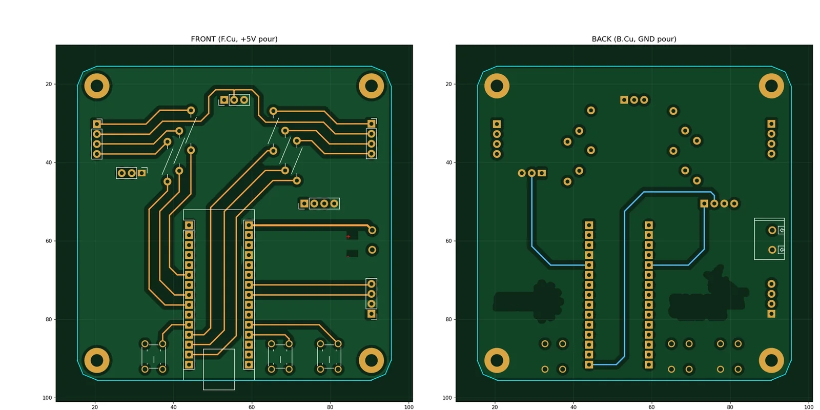
Three zones total. Because both rails are planes, no power tracks were routed: every
module header, every LED cathode return and all four mounting-hole pads pick up their
rail from the nearest plane. H1–H4 are MountingHole_Pad footprints with plated pads
tied to GND, so metal standoffs bond the frame to ground.
Signal routing: 90 track segments, predominantly 1.0 mm wide with a few at 0.5 mm and 1.5 mm. That is far wider than the ~50 mA these signals carry; the width is chosen so the tracks are visible and probe-able by students, not for current capacity.
4. Design rules as shipped
From campv2.kicad_pro:
| Rule | Value |
|---|---|
| Minimum track width | 0.5 mm |
| Minimum clearance | 0.5 mm |
| Minimum through-hole diameter | 0.3 mm |
| Minimum via diameter / drill | 0.5 mm / 0.3 mm |
| Copper-to-edge clearance | 0.5 mm |
| Hole-to-hole | 0.25 mm |
| Minimum silkscreen text height | 0.8 mm |
| Default netclass track / via | 0.2 mm / 0.6 mm ⌀, 0.3 mm drill |
| Preset track widths | 0.5, 1.0, 1.5 mm |
Every one of these is well inside the capability of the cheapest 2-layer service, which is the point — the board is meant to be ordered in class quantities from whoever is fastest, not whoever is most capable.
5. Repository conventions
Library resolution
Both library tables are project-relative and therefore machine-independent:
; campv2/sym-lib-table
(lib (name "easyeda2kicad") (type "KiCad")
     (uri "${KIPRJMOD}/../lib/lcsc/easyeda2kicad.kicad_sym"))

; campv2/fp-lib-table
(lib (name "easyeda2kicad") (type "KiCad")
     (uri "${KIPRJMOD}/../lib/lcsc/easyeda2kicad.pretty"))
(lib (name "production")    (type "KiCad")
     (uri "${KIPRJMOD}/../production"))
${KIPRJMOD} expands to the directory containing the .kicad_pro, so both entries
resolve wherever the repository is cloned. Note the second footprint entry: the two logo
footprints on B.Silkscreen were placed from a library nicknamed production, and the
footprint instances inside campv2.kicad_pcb still carry that nickname, so the nickname
has to stay exactly that. It points at the top-level production/ folder, which is where
the .kicad_mod files live. That folder does not carry the conventional .pretty
suffix; KiCad reads it anyway, but if you ever want it to be textbook-correct, rename it
to production.pretty and change the URI to match — the nickname stays production
either way.
3D model paths in the PCB likewise use ${KIPRJMOD}/../lib/3d/…,
${KIPRJMOD}/../lib/lcsc/… and ${KICAD10_3DMODEL_DIR}/….
No user-defined path variables are required.
If you add a library, add it to the project table, not the global one. A global entry works on your machine and breaks for everyone who clones the repository.
Adding a part from LCSC
pip install easyeda2kicad
# append the LCSC code (e.g. C2837020) to lcsc.txt, then:
python lcsc.py lcsc.txt ./lib/lcsc
This pulls the symbol, footprint and 3D model straight into lib/lcsc/, where the
project tables already point. Codes currently in use:
| LCSC | Part |
|---|---|
C2837020 |
TJ-L5FCMXHTCSLCRGB-A5 — 4-pin RGB LED |
C2837515 |
KH-6X6X5H-TJ — 6 × 6 × 5 mm tactile switch |
C5371917 |
DEGSON DG301-5.0-02P — 2-way 5 mm screw terminal |
Regenerating production files
The campv2/production/ outputs were generated by the KiCad Fabrication Toolkit
plugin; its settings are stored in campv2/fabrication-toolkit-options.json.
Re-running the plugin reproduces the gerber zip, bom.csv, positions.csv,
designators.csv and netlist.ipc in one step.
Do not hand-edit anything in campv2/production/. It is generated output. If a value there
is wrong, the schematic or the layout is wrong.
6. What lives in archive/
| Folder | What it was |
|---|---|
camp/ |
TechnoCamp2026 CubeSat rev A, 2026-08-07. Same concept, eight resistors (R4–R11) instead of six. Superseded by v2 before any boards were made. |
camp_demo/ |
TechnoCamp2026Demo — a minimal teaching board: one Arduino Nano footprint and one RGB LED. Used to demonstrate the KiCad workflow from scratch in a single session. |
camp_t9/ |
An empty KiCad project (Cubesat rev A, 2026-08-18): no symbols, no footprints, a 79-byte PCB file. A "File → New Project" stub that never got any content. |
The earlier vector traces of the two silkscreen logos, and the PNG/JPG artwork they were
made from, sit alongside the live ones in the top-level production/ folder. Only
turin_logo2 and assotsiatsiya_logo are on the board.
7. Known issues
1 — Reference designators differ between the schematic and the PCB. The board was re-annotated in the layout editor without back-annotating the schematic. The link is intact — all 21 footprints still match their schematic symbols by UUID — but the visible names differ:
| Schematic | PCB / silkscreen / BOM |
|---|---|
A2 |
ARDUINO1 |
J2 |
DHT11 |
J3 |
LCD |
J4 |
MQ-7 |
LED2 |
LED1 |
LED3 |
LED2 |
Everything else (R4–R9, SW1–SW3, U1, J5, H1–H4) matches.
⚠️ Do not run Tools → Update PCB from Schematic on this project without checking the preview. KiCad will rename the footprints back to the schematic's designators, which silently invalidates the silkscreen you have already had manufactured and every reference in
bom.csv,positions.csvand the firmware comments.The clean fix is to re-annotate the schematic to match the board (right-click each symbol → Properties, or Tools → Annotate with the PCB as the source), then run the update. That is a rev-C task; the shipped rev B is consistent with itself everywhere that matters — silkscreen, BOM, pick-and-place and firmware all use the PCB names.
2 — The MQ-7 pin legend on the schematic is transposed.
The text annotation beside J4 reads, top to bottom, DOUT / AOUT / GND / VCC. Pins 3
and 4 are correct (GND, +5V), but pins 1 and 2 are the wrong way round: pin 1 is wired
to A7, which on an ATmega328P in the Nano package is an analogue input with no digital
input buffer at all and therefore can only be the sensor's analogue output. Pin 2 goes
to D12, the digital output. The firmware has it right (PIN_MQ7_ANALOG = A7,
PIN_MQ7_ALARM = 12); only the drawing's caption is wrong.
This is cosmetic — no copper is affected — but it should be corrected in the schematic before the next class, because a student reading the schematic will wire their MQ-7 module backwards. MQ-7 breakout modules also vary in pin order between suppliers, so check the silkscreen on the module itself.
3 — No power-input protection. See §3.
8. Ideas for a rev C
Ordered by how much they would improve the class, not by difficulty:
- Reverse-polarity and ORing protection on
VCC, so a student cannot cook a Nano by powering it from USB and the terminal at once. - Back-annotate the designators so the schematic and the board agree (§7.1), and fix the MQ-7 caption (§7.2).
- Per-pin silkscreen labels on the DHT11, MQ-7 and LCD headers. The pin functions are
currently only on the schematic; putting
GND VCC SDA SCLnext to the LCD header would remove the most common wiring mistake at the bench. - Break the five free pins out (
D4,D7,A2,A3,A6) to a 1×5 header with a GND and a 5 V pin beside it, so students can add their own sensor. - Test points on
+5V,VCCandGND— teaching multimeter use is much easier with somewhere to put the probe. - A DHT22-compatible footprint — same 3 pins, so this costs nothing but a silkscreen note.
9. Toolchain
| Tool | Version | Used for |
|---|---|---|
| KiCad | 10.0 | Schematic and layout |
| KiCad Fabrication Toolkit | — | Gerber / BOM / CPL generation |
easyeda2kicad |
— | Importing LCSC parts, via lcsc.py |
| Arduino IDE | 1.8 or 2.x | Building and flashing the firmware |
Anything older than KiCad 9 cannot open these files.